February 28, 2024
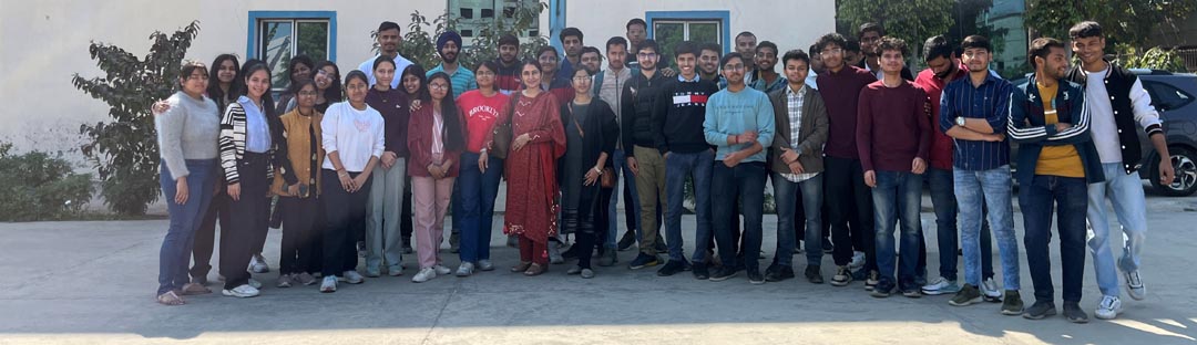
3 days PCB Designing workshop for students was organised by GTBIT and the R&D team of C-DAC Noida .
Showcasing the state-of-the-art facilities at C-DAC Noida's lab, equipped with advanced computing resources, electronic design tools, and industry- standard PCB fabrication capabilities, providing an optimal learning environment for the participants.

* Expert-Led Sessions on multistable and monostable vibrator design, semantic layering, and practical PCB design exercises, provide participants with valuable insights and hands-on experience, ensuring comprehensive skill development.
* These programs were designed to align with industry requirements, ensuring that participants are well-prepared for real-world applications of PCB designing.